BRAIN BOXES
OPTO DIO 48 (VER. 4.0)
|
Card Type |
Digital I/O card |
|
Chip Set |
Unidentified |
|
I/O Options |
50-pin connector |
|
Data Bus |
16-bit ISA |
|
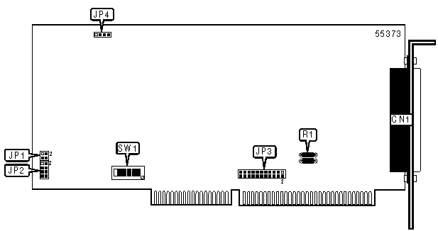
CONNECTIONS | |
|
Function |
Label |
|
50-pin connector |
CN1 |
|
USER CONFIGURABLE SETTINGS | |||
|
Function |
Label |
Position | |
| » |
UDN2984 Source drivers selected |
R1 |
Resistors installed |
|
ULN2804 Sink drivers selected |
R1 |
Resistors removed | |
|
WATCHDOG OUTPUT SELECTION | |||
|
Function |
Label |
Position | |
|
Reslo bus |
JP1 |
Pins 1 & 2 closed | |
| » |
Reshi bus |
JP1 |
Pins 3 & 4 closed |
|
Reshi out |
JP2 |
Pins 1 & 2 closed | |
|
Reslo out |
JP2 |
Pins 2 & 3 closed | |
| » |
Goodlo out |
JP2 |
Pins 3 & 4 closed |
|
Goodhi out |
JP2 |
Pins 5 & 6 closed | |
| » |
Port A1 bit 0 output |
JP4 |
Pins 1 & 2 closed |
|
Watchdog out signal output |
JP4 |
Pins 2 & 3 closed | |
|
SERIAL PORT 1 INTERRUPT SELECTION | |
|
IRQ |
JP3 |
|
2 |
Pins 11 & 12 closed |
|
3 |
Pins 9 & 10 closed |
|
4 |
Pins 7 & 8 closed |
|
5 |
Pins 5 & 6 closed |
|
6 |
Pins 3 & 4 closed |
|
7 |
Pins 1 & 2 closed |
|
10 |
Pins 13 & 14 closed |
|
11 |
Pins 15 & 16 closed |
|
12 |
Pins 17 & 18 closed |
|
15 |
Pins 21 & 22 closed |
|
BASE I/O ADDRESS SELECTION | |||||||
|
Setting |
SW1/1 |
SW1/2 |
SW1/3 |
SW1/4 |
SW1/5 |
SW1/6
| |
|
200h |
On |
On |
On |
On |
On |
On | |
|
208h |
Off |
On |
On |
On |
On |
On | |
|
210h |
On |
Off |
On |
On |
On |
On | |
|
218h |
Off |
Off |
On |
On |
On |
On | |
|
220h |
On |
On |
Off |
On |
On |
On | |
| » |
308h |
Off |
On |
On |
On |
On |
Off |
|
3D8h |
Off |
Off |
On |
Off |
Off |
Off | |
|
3E0h |
On |
On |
Off |
Off |
Off |
Off | |
|
3E8h |
Off |
On |
Off |
Off |
Off |
Off | |
|
3F0h |
On |
Off |
Off |
Off |
Off |
Off | |
|
3F8h |
Off |
Off |
Off |
Off |
Off |
Off | |
|
Note: A total of 64 base address settings are available. The switches are a binary representation of the decimal memory addresses. SW1/6 is the Most Significant Bit and switch SW1/1 is the Least Significant Bit. The switches have the following decimal values: SW1/6=512, SW1/5=128, SW1/4=64, SW1/3=32, SW1/2=16, SW1/1=8. Turn off the switches and add the values of the switches to obtain the correct memory address. (Off=1, On=0) | |||||||