ADVANCED INTEGRATION RESEARCH, INC.
54CPI (REV. 3.00)
|
Processor |
Pentium |
|
Processor Speed |
75/90/100/120/133/150/166MHz |
|
Chip Set |
Intel |
|
Video Chip Set |
None |
|
Maximum Onboard Memory |
128MB (EDO supported) |
|
Maximum Video Memory |
None |
|
Cache |
256/512KB |
|
BIOS |
Unidentified |
|
Dimensions |
330mm x 222mm |
|
I/O Options |
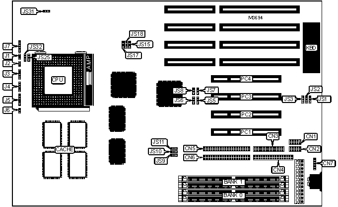
32-bit PCI slots (4), floppy drive interface, green PC connector, IDE interfaces (2), parallel port, PS/2 mouse interface, serial ports (2), IR connector |
|
NPU Options |
None |
|
CONNECTIONS | |||
|
Purpose |
Location |
Purpose |
Location |
|
Serial port 1 |
CN1 |
Reset switch |
J2 |
|
Serial port 2 |
CN2 |
Speaker |
J3 |
|
Parallel port |
CN3 |
IDE interface LED |
J4 |
|
Floppy drive interface |
CN4 |
Power LED & keylock |
J5 |
|
IDE interface 2 |
CN5 |
Turbo LED |
J6 |
|
IDE interface 1 |
CN6 |
IR connector |
J7 |
|
PS/2 mouse interface |
CN7 |
32-bit PCI slots |
PC1 - PC4 |
|
Green PC connector |
J1 | ||
|
USER CONFIGURABLE SETTINGS | |||
|
Function |
Label |
Position | |
|
» |
Factory configured - do not alter |
JS3 |
Unidentified |
|
» |
Parallel port IRQ select IRQ7 |
JS5 |
Pins 1 & 2 closed |
|
Parallel port IRQ select IRQ5 |
JS5 |
Pins 2 & 3 closed | |
|
» |
Monitor type select monochrome/EGA/VGA |
JS15 |
Pins 2 & 3 closed |
|
Monitor type select CGA |
JS15 |
Pins 1 & 2 closed | |
|
» |
Flash BIOS voltage select 12v |
JS17 |
Pins 1 & 2 closed |
|
Flash BIOS voltage select 5v |
JS17 |
Pins 2 & 3 closed | |
|
» |
CMOS memory normal operation |
JS18 |
Pins 1 & 2 closed |
|
CMOS memory clear |
JS18 |
Pins 2 & 3 closed | |
|
DRAM CONFIGURATION | ||
|
Size |
Bank 0 |
Bank 1 |
|
8MB |
(2) 1M x 36 |
None |
|
16MB |
(2) 2M x 36 |
None |
|
16MB |
(2) 1M x 36 |
(2) 1M x 36 |
|
24MB |
(2) 1M x 36 |
(2) 2M x 36 |
|
32MB |
(2) 4M x 36 |
None |
|
32MB |
(2) 2M x 36 |
(2) 2M x 36 |
|
40MB |
(2) 1M x 36 |
(2) 4M x 36 |
|
48MB |
(2) 2M x 36 |
(2) 4M x 36 |
|
64MB |
(2) 8M x 36 |
None |
|
64MB |
(2) 4M x 36 |
(2) 4M x 36 |
|
72MB |
(2) 1M x 36 |
(2) 8M x 36 |
|
80MB |
(2) 2M x 36 |
(2) 8M x 36 |
|
96MB |
(2) 4M x 36 |
(2) 8M x 36 |
|
128MB |
(2) 8M x 36 |
(2) 8M x 36 |
|
Note: Board accepts EDO memory. Board also accepts x 32 SIMMs. | ||
|
CACHE CONFIGURATION | ||
|
Size |
Bank 0 |
Bank 1 |
|
256KB |
(2) 32K x 32 |
None |
|
512KB |
(2) 32K x 32 |
(2) 32K x 32 |
|
Note: The location of banks 0 & 1 are unidentified. | ||
|
CPU SPEED SELECTION | |||||||
|
CPU speed |
Clock speed |
Multiplier |
JS9 |
JS10 |
JS11 |
JS25 |
JS32 |
|
75MHz |
50MHz |
1.5x |
1 & 2 |
2 & 3 |
1 & 2 |
1 & 2 |
1 & 2 |
|
90MHz |
60MHz |
1.5x |
1 & 2 |
1 & 2 |
2 & 3 |
1 & 2 |
1 & 2 |
|
100MHz |
66MHz |
1.5x |
2 & 3 |
2 & 3 |
2 & 3 |
1 & 2 |
1 & 2 |
|
120MHz |
60MHz |
2x |
1 & 2 |
1 & 2 |
2 & 3 |
1 & 2 |
2 & 3 |
|
133MHz |
66MHz |
2x |
2 & 3 |
2 & 3 |
2 & 3 |
1 & 2 |
2 & 3 |
|
150MHz |
60MHz |
2.5x |
1 & 2 |
1 & 2 |
2 & 3 |
2 & 3 |
2 & 3 |
|
166MHz |
66MHz |
2.5x |
2 & 3 |
2 & 3 |
2 & 3 |
2 & 3 |
2 & 3 |
|
Note: Pins designated should be in the closed position. | |||||||
|
CPU VOLTAGE SELECTION | ||
|
Voltage |
JS31 | |
| » |
STD/VR |
Pins 2 & 3 closed |
|
VRE |
Pins 1 & 2 closed | |
|
DMA CHANNEL SELECTION | ||||
|
Channel |
JS1 |
JS7 |
JS8 | |
| » |
Normal |
Pins 2 & 3 closed |
Open |
Open |
|
1 |
Pins 1 & 2 closed |
Pins 2 & 3 closed |
Pins 2 & 3 closed | |
|
3 |
Pins 1 & 2 closed |
Pins 1 & 2 closed |
Pins 1 & 2 closed | |
|
FLOPPY DRIVE SELECTION | |||
|
Setting |
JS2 |
JS6 | |
| » |
Normal |
Pins 2 & 3 closed |
Open |
|
Enhanced |
Pins 1 & 2 closed |
Pins 2 & 3 closed | |