NIAGARA SMD TECHNOLOGY, INC.
NT924 REV-PB CACHE
|
Processor |
CX M1/AM K5/IBM/SGS/Thompson/Pentium |
|
Processor Speed |
75/90/100/120/133/150/166/180/200MHz |
|
Chip Set |
Intel |
|
Maximum Onboard Memory |
128MB |
|
Cache |
256/512KB |
|
BIOS |
Award/Phoenix |
|
Dimensions |
330mm x 218mm |
|
I/O Options |
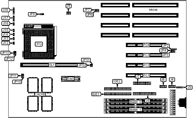
32-bit PCI slots (4), floppy drive interface, green PC connector, IDE interfaces (2), parallel port, PS/2 mouse interface, serial ports (2), cache slot |
|
NPU Options |
None |
|
CONNECTIONS | |||
|
Function |
Label |
Function |
Label |
|
IDE interface 1 |
IDE1 |
IDE interface LED |
J13 |
|
IDE interface 2 |
IDE2 |
Green PC LED |
J14 |
|
PS/2 mouse interface |
J3 |
Turbo LED |
J15 |
|
Serial port 1 |
J4 |
Reset switch |
J16 |
|
Serial port 2 |
J6 |
Speaker |
J17 |
|
Floppy drive interface |
J7 |
Power LED & keylock |
J18 |
|
Parallel port |
J8 |
32-bit PCI slots |
PC1 - PC4 |
|
chassis fan power |
J9 |
Cache slot |
SL1 |
|
Green PC connector |
J12 | ||
|
USER CONFIGURABLE SETTINGS | |||
|
Setting |
Label |
Position | |
|
Jumper information unavailable |
JP2 |
N/A | |
|
Keyboard clock select depends on ISA clock |
JP4 |
Pins 1 & 2 closed | |
|
Keyboard clock select set at 12MHz |
JP4 |
Pins 2 & 3 closed | |
|
Jumper information unavailable |
JP6 |
N/A | |
|
» |
Flash BIOS voltage select 5v |
JP7 |
Pins 1 & 2 closed |
|
Flash BIOS voltage select 12v |
JP7 |
Pins 2 & 3 closed | |
|
DRAM | ||
|
Size |
Bank 0 |
Bank 1 |
|
8MB |
(2) 1M x 32 |
None |
|
8MB |
(2) 512K x 32 |
(2) 512K x 32 |
|
10MB |
(2) 1M x 32 |
(2) 256K x 32 |
|
10MB |
(2) 256K x 32 |
(2) 1M x 32 |
|
12MB |
(2) 1M x 32 |
(2) 512K x 32 |
|
12MB |
(2) 512K x 32 |
(2) 1M x 32 |
|
16MB |
(2) 2M x 32 |
None |
|
16MB |
(2) 1M x 32 |
(2) 1M x 32 |
|
18MB |
(2) 2M x 32 |
(2) 256K x 32 |
|
18MB |
(2) 256K x 32 |
(2) 2M x 32 |
|
20MB |
(2) 2M x 32 |
(2) 512K x 32 |
|
20MB |
(2) 512K x 32 |
(2) 2M x 32 |
|
24MB |
(2) 2M x 32 |
(2) 1M x 32 |
|
24MB |
(2) 1M x 32 |
(2) 2M x 32 |
|
32MB |
(2) 4M x 32 |
None |
|
32MB |
(2) 2M x 32 |
(2) 2M x 32 |
|
34MB |
(2) 4M x 32 |
(2) 256K x 32 |
|
34MB |
(2) 256K x 32 |
(2) 4M x 32 |
|
36MB |
(2) 4M x 32 |
(2) 512K x 32 |
|
36MB |
(2) 512K x 32 |
(2) 4M x 32 |
|
40MB |
(2) 4M x 32 |
(2) 1M x 32 |
|
40MB |
(2) 1M x 32 |
(2) 4M x 32 |
|
48MB |
(2) 4M x 32 |
(2) 2M x 32 |
|
48MB |
(2) 2M x 32 |
(2) 4M x 32 |
|
64MB |
(2) 8M x 32 |
None |
|
64MB |
(2) 4M x 32 |
(2) 4M x 32 |
|
66MB |
(2) 8M x 32 |
(2) 256K x 32 |
|
66MB |
(2) 256K x 32 |
(2) 8M x 32 |
|
68MB |
(2) 8M x 32 |
(2) 512K x 32 |
|
68MB |
(2) 512K x 32 |
(2) 8M x 32 |
|
72MB |
(2) 8M x 32 |
(2) 1M x 32 |
|
72MB |
(2) 1M x 32 |
(2) 8M x 32 |
|
DRAM | ||
|
Size |
Bank 0 |
Bank 1 |
|
80MB |
(2) 8M x 32 |
(2) 2M x 32 |
|
80MB |
(2) 2M x 32 |
(2) 8M x 32 |
|
96MB |
(2) 8M x 32 |
(2) 4M x 32 |
|
96MB |
(2) 4M x 32 |
(2) 8M x 32 |
|
128MB |
(2) 8M x 32 |
(2) 8M x 32 |
|
Note: Board accepts EDO memory. Board also accepts x 36 SIMMs. | ||
|
CACHE SIZE | ||||
|
Size |
Bank 0 |
Bank 1 |
TAG |
SL1 |
|
256KB (A) |
256KB |
None |
(1) 8K/16K x 8 |
Not installed |
|
256KB (B) |
None |
None |
None |
Installed |
|
512KB (A) |
256KB |
256KB |
(1) 16K/32K x 8 |
Not installed |
|
512KB (B) |
None |
None |
None |
Installed |
|
Note: The orientation of banks 0 & 1 is unidentified. | ||||
|
CACHE JUMPER | ||
|
Size |
JP10 |
JP11 |
|
256KB (A/B) |
Pins 1 & 2 closed |
Pins 1 & 2 closed |
|
512KB (A/B) |
Pins 2 & 3 closed |
Pins 2 & 3 closed |
|
CPU TYPE | |
|
Setting |
JP8 |
|
CX M1 |
Pins 1 & 2 closed |
|
AM K5 |
Pins 1 & 2 closed |
|
P54C |
Pins 1 & 2 closed |
|
P55C (reserved for future upgrade) |
Pins 2 & 3 closed |
|
CPU SPEED (INTEL) | |||||
|
Setting |
JP3 |
JP12 |
JP13 |
JPS1 |
JPS2 |
|
75MHz |
1 & 2 |
2 & 3 |
2 & 3 |
Closed |
Closed |
|
90MHz |
2 & 3 |
2 & 3 |
2 & 3 |
Open |
Open |
|
100MHz |
2 & 3 |
2 & 3 |
2 & 3 |
Open |
Closed |
|
120MHz |
2 & 3 |
2 & 3 |
1 & 2 |
Closed |
Open |
|
133MHz |
2 & 3 |
2 & 3 |
1 & 2 |
Open |
Closed |
|
150MHz |
2 & 3 |
1 & 2 |
1 & 2 |
Closed |
Open |
|
166MHz |
2 & 3 |
1 & 2 |
1 & 2 |
Open |
Closed |
|
180MHz |
2 & 3 |
1 & 2 |
2 & 3 |
Closed |
Open |
|
200MHz |
2 & 3 |
1 & 2 |
2 & 3 |
Open |
Closed |
|
Note: Pins designated should be in the closed position. | |||||
|
CPU SPEED(CYRIX/IBM/SGS/THOMPSON) | |||||
|
Setting |
JP3 |
JP12 |
JP13 |
JPS1 |
JPS2 |
|
100MHz |
1 & 2 |
2 & 3 |
1 & 2 |
Closed |
Closed |
|
120MHz |
2 & 3 |
2 & 3 |
1 & 2 |
Closed |
Open |
|
133MHz |
1 & 2 |
2 & 3 |
1 & 2 |
Open |
Open |
|
Note: Pins designated should be in the closed position. | |||||