TANDON CORPORATION
MODEL 189370/199720
|
Processor |
80286 |
|
Processor Speed |
6/8/10MHz |
|
Chip Set |
Unidentified |
|
Maximum Onboard Memory |
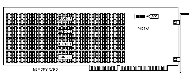
3MB (2.5MB on external memory card) |
|
Cache |
None |
|
BIOS |
Unidentified |
|
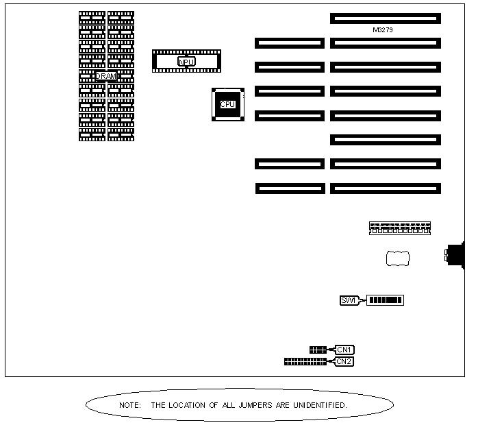
Dimensions |
355mm x 305mm |
|
I/O Options |
Serial port, parallel port |
|
NPU Options |
80287 |
|
CONNECTIONS | |||
|
Function |
Label |
Function |
Label |
|
Serial port |
CN1 |
Parallel port |
CN2 |
|
USER CONFIGURABLE SETTINGS | |||
|
Setting |
Label |
Position | |
|
Signal select DTR driven |
JP1 |
Pins 1 & 2 closed | |
|
Signal select DTR true |
JP1 |
Pins 2 & 3 closed | |
|
Signal select DTR false |
JP1 |
Open | |
|
Signal select RTS driven |
JP2 |
Pins 1 & 2 closed | |
|
Signal select RTS true |
JP2 |
Pins 2 & 3 closed | |
|
Signal select RTS false |
JP2 |
Open | |
|
Signal select DCD driven |
JP3 |
Pins 1 & 2 closed | |
|
Signal select DCD true |
JP3 |
Pins 2 & 3 closed | |
|
Signal select DCD false |
JP3 |
Open | |
|
Signal select DSR driven |
JP4 |
Pins 1 & 2 closed | |
|
Signal select DSR true |
JP4 |
Pins 2 & 3 closed | |
|
Signal select DSR false |
JP4 |
Open | |
|
Signal select CTS driven |
JP5 |
Pins 1 & 2 closed | |
|
Signal select CTS true |
JP5 |
Pins 2 & 3 closed | |
|
Signal select CTS false |
JP5 |
Open | |
|
» |
Factory configured - do not alter (189370-001, 002) |
JP6 |
Open |
|
» |
Factory configured - do not alter (189370-004, 005/199270) |
JP6 |
Open |
|
» |
Factory configured - do not alter (189370-001, 002) |
JP7 |
Open |
|
» |
Factory configured - do not alter (189370-004, 005/199270 |
JP7 |
Pins 1 & 2 closed |
|
» |
Factory configured - do not alter (189370-001, 002) |
JP8 |
Pins 2 & 3 closed |
|
» |
Factory configured - do not alter (189370-004, 005/199270) |
JP8 |
Pins 1 & 2 closed |
|
» |
Factory configured - do not alter (189370-001, 002) |
JP9 |
Pins 2 & 3 closed |
|
» |
Factory configured - do not alter (189370-004, 005/199270) |
JP9 |
Pins 1 & 2 closed |
|
» |
Factory configured - do not alter (189370-001, 002) |
JP10 |
Pins 1 & 2 closed |
|
» |
Factory configured - do not alter (189370-004, 005/199270) |
JP10 |
Open |
|
» |
Factory configured - do not alter (189370-001, 002) |
JP11 |
Pins 1 & 2 closed |
|
» |
Factory configured - do not alter (189370-004, 005/199270) |
JP11 |
Pins 1 & 2 closed |
|
» |
Factory configured - do not alter (189370-001, 002) |
JP12 |
Open |
|
» |
Factory configured - do not alter (189370-004, 005/199270) |
JP12 |
Open |
|
» |
Factory configured - do not alter (189370-001, 002) |
JP13 |
Pins 1 & 2 closed |
|
» |
Factory configured - do not alter (189370-004, 005/199270) |
JP13 |
Pins 1 & 2 closed |
|
» |
Factory configured - do not alter (189370-001, 002) |
JP14 |
Pins 2 & 3 closed |
|
» |
Factory configured - do not alter (189370-004, 005/199270) |
JP14 |
Pins 1 & 2 closed |
|
0 wait state enabled (model 199720 only) |
SW1/1 |
On | |
|
0 wait state disabled (model 199720 only) |
SW1/1 |
Off | |
|
» |
Factory configured - do not alter |
SW1/2 |
N/A |
|
» |
Video type select 80 characters |
SW1/3 |
Off |
|
» |
Factory configured - do not alter |
SW1/4 |
Off |
|
USER CONFIGURABLE SETTINGS (CON’T) | |||
|
Setting |
Label |
Position | |
|
» |
Factory configured - do not alter |
SW1/5 |
N/A |
|
» |
Factory configured - do not alter |
SW1/6 |
N/A |
|
» |
Factory configured - do not alter |
SW1/7 |
N/A |
|
512KB - 640KB RAM address enabled |
SW1/8 |
On | |
|
512KB - 640KB RAM address disabled |
SW1/8 |
Off | |
|
DRAM |
|
Note: The orientation and chip sizes are unidentified. |
|
DRAM | ||||
|
Size |
Bank 0 |
Bank 1 |
Bank 2 |
Bank 3 |
|
512KB |
(18) 41256 |
None |
None |
None |
|
1MB |
(18) 41256 |
(18) 41256 |
None |
None |
|
1.5MB |
(18) 41256 |
(18) 41256 |
(18) 41256 |
None |
|
2MB |
(18) 41256 |
(18) 41256 |
(18) 41256 |
(18) 41256 |
|
DRAM SWITCH | ||||||
|
Memory before |
Memory after |
SW1/1 |
SW1/2 |
SW1/3 |
SW1/4 |
SW1/5 |
|
512-640KB |
2560-2688KB |
Off |
Off |
Off |
On |
Off |
|
1024KB |
3072KB |
Off |
Off |
Off |
On |
On |
|
2560-2688KB |
4608-4736KB |
Off |
Off |
On |
On |
Off |
|
3072KB |
5120KB |
Off |
Off |
On |
On |
On |
|
4608-4736KB |
6656-6784KB |
Off |
On |
Off |
On |
Off |
|
5120KB |
7168KB |
Off |
On |
Off |
On |
On |
|
656-6784KB |
8704-8832KB |
Off |
On |
On |
On |
Off |
|
7168KB |
9216KB |
Off |
On |
On |
On |
On |
|
DRAM SWITCH (CON’T) | ||||||
|
Memory before |
Memory after |
SW1/1 |
SW1/2 |
SW1/3 |
SW1/4 |
SW1/5 |
|
8704-8832KB |
10752-10880KB |
On |
Off |
Off |
On |
Off |
|
9216KB |
11264KB |
On |
Off |
Off |
On |
On |
|
10752-10880KB |
12800-12928KB |
On |
Off |
On |
On |
Off |
|
11264KB |
13312KB |
On |
Off |
On |
On |
On |
|
12800-12928KB |
14848-14976KB |
On |
On |
Off |
On |
Off |
|
13312KB |
15360KB |
On |
On |
Off |
On |
On |
|
14848-14976KB |
15744KB |
On |
On |
On |
On |
Off |
|
15360KB |
15744KB |
On |
On |
On |
On |
On |
|
MISCELLANEOUS TECHNICAL NOTE |
|
The location of pin 1 is unidentified. |